4. Hardware Guide
4.1. About this Chapter
This Hardware Guide provides information about the features, connectors and signals available on the A31 µQ7 module.
Note
This chapter describes the µQ7 module itself. See chapter 2 Using the EVK for details on the baseboard.
4.2. Qseven Implementation
Qseven has mandatory and optional features. Following table shows the feature set of the A31 µQ7 module compared to the minimum ARM/RISC based and maximum configuration.
| System I/O Interface | ARM/RISC Based Minimum Configuration | A31 µQ7 | Maximum Configuration |
|---|---|---|---|
| PCI Express lanes | 0 | 0 | 4 |
| Serial ATA channels | 0 | 1 | 2 |
| USB 2.0 ports | 3 | 8 | 8 |
| USB 3.0 ports | 0 | 0 | 2 |
| LVDS channels embedded DisplayPort | 0 | Dual Channel LVDS | Dual Channel 2 |
| DisplayPort, TMDS | 0 | 1 (HDMI) | 1 |
| High Definition Audio / AC‘97 / I2S | 0 | 0/0/1 | 1 |
| Ethernet 10/100 Mbit/Gigabit | 0 | 1 (Gigabit) | 1 (Gigabit) |
| UART | 0 | 1 | 1 |
| Low Pin Count bus / GPIO | 0 | 0/8 (GPIO) | 1 |
| Secure Digital I/O 8-bit for SD/MMC cards | 0 | 1 (4-bit SD-Card) | 1 |
| System Management Bus | 0 | 1 | 1 |
| I²C Bus | 1 | 1 | 1 |
| SPI Bus | 0 | 1 | 1 |
| CAN Bus | 0 | 1 | 1 |
| Watchdog Trigger | 1 | 1 | 1 |
| Power Button | 1 | 1 | 1 |
| Power Good | 1 | 1 | 1 |
| Reset Button | 1 | 1 | 1 |
| LID Button | 0 | 1 | 1 |
| Sleep Button | 0 | 1 | 1 |
| Suspend To RAM (S3 mode) | 0 | 1 | 1 |
| Wake | 0 | 1 | 1 |
| Battery low alarm | 0 | 1 | 1 |
| Thermal control | 0 | 1 | 1 |
| FAN control | 0 | 1 | 1 |
Note
The A31 µQ7 module is available in different variants. This document describes the maximum configuration. For details about orderable variants please refer to the the order-code document.
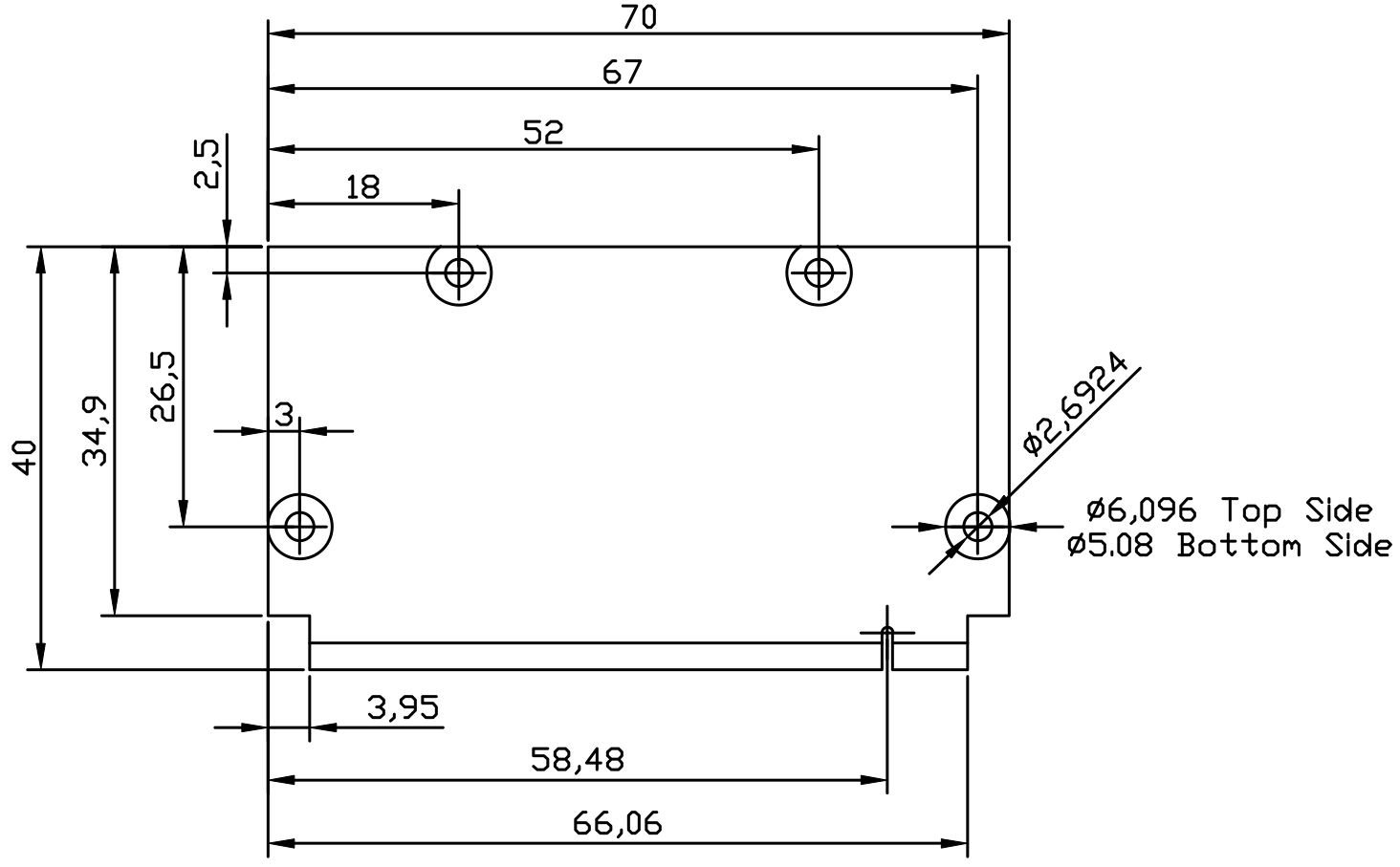
4.3. Connector Description
The following table shows the signals on the edge connector of the A31 µQ7 module.
Empty cells are not connected (NC) pins.
| Pin | Signal | Pin | Signal |
|---|---|---|---|
| 1 | GND | 2 | GND |
| 3 | GBE_MDI3- | 4 | GBE_MDI2- |
| 5 | GBE_MDI3+ | 6 | GBE_MDI2+ |
| 7 | GBE_LINK100# | 8 | GBE_LINK1000# |
| 9 | GBE_MDI1- | 10 | GBE_MDIO0- |
| 11 | GBE_MDI1+ | 12 | GBE_MDIO0+ |
| 13 | GBE_LINK# | 14 | GBE_ACT# |
| 15 | GBE_CTREF | 16 | SUS_S5# |
| 17 | WAKE# | 18 | SUS_S3# |
| 19 | SUS_STAT# | 20 | PWRBTN# |
| 21 | SLP_BTN# | 22 | LID_BTN# |
| 23 | GND | 24 | GND |
| 25 | GND | 26 | PWGIN |
| 27 | BATLOW# | 28 | RSTBTN# |
| 29 | SATA0_TX+ | 30 | |
| 31 | SATA0_TX- | 32 | |
| 33 | SATA_ACT# | 34 | GND |
| 35 | SATA0_RX+ | 36 | |
| 37 | SATA0_RX- | 38 | |
| 39 | GND | 40 | GND |
| 41 | BIOS_DISABLE# / BOOT_ALT# | 42 | SDIO_CLK# |
| 43 | SDIO_CD# | 44 | SDIO_LED |
| 45 | SDIO_CMD | 46 | SDIO_WP |
| 47 | SDIO_PWR# | 48 | SDIO_DAT1 |
| 49 | SDIO_DAT0 | 50 | SDIO_DAT3 |
| 51 | SDIO_DAT2 | 52 | |
| 53 | 54 | ||
| 55 | 56 | ||
| 57 | GND | 58 | GND |
| 59 | I2S_WS | 60 | SMB_CLK / GP1_I2C_CLK |
| 61 | I2S_RST# | 62 | SMB_DAT / GP1_I2C_DAT |
| 63 | I2S_CLK | 64 | SMB_ALERT# |
| 65 | I2S_SDI | 66 | GP0_I2C_CLK |
| 67 | I2S_SDO | 68 | GP0_I2C_DAT |
| 69 | THRM# | 70 | WDTRIG# |
| 71 | THRMTRIP# | 72 | WDOUT |
| 73 | GND | 74 | GND |
| 75 | USB_P7- | 76 | USB_P6- |
| 77 | USB_P7+ | 78 | USB_P6+ |
| 79 | USB_6_7_OC# | 80 | USB_4_5_OC# |
| 81 | USB_P5- | 82 | USB_P4- |
| 83 | USB_P5+ | 84 | USB_P4+ |
| 85 | USB_2_3_OC# | 86 | USB_0_1_OC# |
| 87 | USB_P3- | 88 | USB_P2- |
| 89 | USB_P3+ | 90 | USB_P2+ |
| 91 | USB_CC | 92 | USB_ID |
| 93 | USB_P1- | 94 | USB_P0- |
| 95 | USB_P1+ | 96 | USB_P0+ |
| 97 | GND | 98 | GND |
| 99 | LVDS_A0+ | 100 | LVDS_B0+ |
| 101 | LVDS_A0- | 102 | LVDS_B0- |
| 103 | LVDS_A1+ | 104 | LVDS_B1+ |
| 105 | LVDS_A1- | 106 | LVDS_B1- |
| 107 | LVDS_A2+ | 108 | LVDS_B2+ |
| 109 | LVDS_A2- | 110 | LVDS_B2- |
| 111 | LVDS_PPEN | 112 | LVDS_BLEN |
| 113 | LVDS_A3+ | 114 | LVDS_B3+ |
| 115 | LVDS_A3- | 116 | LVDS_B3- |
| 117 | GND | 118 | GND |
| 119 | LVDS_A_CLK+ | 120 | LVDS_B_CLK+ |
| 121 | LVDS_A_CLK- | 122 | LVDS_B_CLK- |
| 123 | LVDS_BLT_CTRL / GP_PWM_OUT0 | 124 | GP_1-Wire_Bus |
| 125 | GP2_I2C_DAT / LVDS_DID_DAT | 126 | LVDS_BLC_DAT |
| 127 | GP2_I2C_CLK / LVDS_DID_CLK | 128 | LVDS_BLC_CLK |
| 129 | CAN0_TX | 130 | CAN0_RX |
| 131 | TMDS_CLK+ | 132 | |
| 133 | TMDS_CLK- | 134 | |
| 135 | GND | 136 | GND |
| 137 | TMDS_LANE1+ | 138 | |
| 139 | TMDS_LANE1- | 140 | |
| 141 | GND | 142 | GND |
| 143 | TMDS_LANE0+ | 144 | |
| 145 | TMDS_LANE0- | 146 | |
| 147 | GND | 148 | GND |
| 149 | TMDS_LANE2+ | 150 | HDMI_CTRL_DAT |
| 151 | TMDS_LANE2- | 152 | HDMI_CTRL_CLK |
| 153 | DP_HDMI_HPD# | 154 | RSVD |
| 155 | 156 | ||
| 157 | 158 | ||
| 159 | GND | 160 | GND |
| 161 | 162 | ||
| 163 | 164 | ||
| 165 | GND | 166 | GND |
| 167 | 168 | ||
| 169 | 170 | ||
| 171 | UART0_TX | 172 | UART0_RTS# |
| 173 | 174 | ||
| 175 | 176 | ||
| 177 | UART0_RX | 178 | UART0_CTS# |
| 179 | 180 | ||
| 181 | 182 | ||
| 183 | GND | 184 | GND |
| 185 | GPIO0 | 186 | LPC_AD1 / GPIO1 |
| 187 | GPIO2 | 188 | LPC_AD3 / GPIO3 |
| 189 | GPIO4 | 190 | LPC_FRAME# / GPIO5 |
| 191 | GPIO6 | 192 | LPC_LDRQ# / GPIO7 |
| 193 | VCC_RTC | 194 | SPKR / GP_PWM_OUT2 |
| 195 | FAN_TACHOIN / GP_TIMER_IN | 196 | FAN_PWMOUT / GP_PWM_OUT1 |
| 197 | GND | 198 | GND |
| 199 | SPI_MOSI | 200 | SPI_CS0# |
| 201 | SPI_MISO | 202 | SPI_CS1# |
| 203 | SPI_SCK | 204 | |
| 205 | VCC_5V_SB | 206 | VCC_5V_SB |
| 207 | JTAG_TCK | 208 | JTAG_TDI |
| 209 | JTAG_TDO | 210 | JTAG_TMS |
| 211 | VCC | 212 | VCC |
| 213 | VCC | 214 | VCC |
| 215 | VCC | 216 | VCC |
| 217 | VCC | 218 | VCC |
| 219 | VCC | 220 | VCC |
| 221 | VCC | 222 | VCC |
| 223 | VCC | 224 | VCC |
| 225 | VCC | 226 | VCC |
| 227 | VCC | 228 | VCC |
| 229 | VCC | 230 | VCC |
4.4. Signal Description
4.4.1. Ethernet
| Signal | Type | Signal Level | Description |
|---|---|---|---|
| GBE_MDI[0:3]+ GBE_MDI[0:3]- | I/O | Analog | Gigabit Ethernet Controller: Media Dependent Interface Differential Pairs 0,1,2,3. The MDI can operate in 1000, 100 and 10 Mbit/sec modes |
| GBE_ACT# | OC | 3.3V | Gigabit Ethernet Controller activity indicator, active low |
| GBE_LINK# | OC | 3.3V | Gigabit Ethernet Controller link indicator, active low |
| GBE_LINK100# | OC | 3.3V | Internaly connected to GBE_LINK# |
| GBE_LINK1000# | OC | 3.3V | Internaly connected to GBE_LINK# |
| GBE_CTREF | REF | Analog | Center Tap Voltage |
4.4.2. SATA
| Signal | Type | Signal Level | Description |
|---|---|---|---|
| SATA0_TX+ SATA0_TX | O | SATA | Serial ATA Channel 0 differential transmit pair |
| SATA0_RX+ SATA0_RX | I | SATA | Serial ATA Channel 0 differential receive pair |
| SATA_ACT# | O | 3.3V | Serial ATA Activity LED |
4.4.3. USB
| Signal | Type | Signal Level | Description |
|---|---|---|---|
| USB_P0+ USB_P0- | I/O | USB | Universal Serial Bus Port 0 differential pair |
| USB_P1+ USB_P1- | I/O | USB | Universal Serial Bus Port 1 differential pair |
| USB_P2+ USB_P2- | I/O | USB | Universal Serial Bus Port 2 differential pair |
| USB_P3+ USB_P3- | I/O | USB | Universal Serial Bus Port 3 differential pair |
| USB_P4+ USB_P4- | I/O | USB | Universal Serial Bus Port 4 differential pair |
| USB_P5+ USB_P5- | I/O | USB | Universal Serial Bus Port 5 differential pair |
| USB_P6+ USB_P6- | I/O | USB | Universal Serial Bus Port 6 differential pair |
| USB_P7+ USB_P7- | I/O | USB | Universal Serial Bus Port 7 differential pair |
| USB_0_1_OC# | I | 3.3V | Over current detect input 1. This pin is used to monitor the USB power over current of the USB Ports 0 and 1 |
| USB_2_3_OC# | I | 3.3V | Over current detect input 1. This pin is used to monitor the USB power over current of the USB Ports 2 and 3 |
| USB_4_5_OC# | I | 3.3V | Over current detect input 1. This pin is used to monitor the USB power over current of the USB Ports 4 and 5 |
| USB_6_7_OC# | I | 3.3V | Over current detect input 1. This pin is used to monitor the USB power over current of the USB Ports 6 and 7 |
| USB_ID | I | 3.3V | Configures the mode of the USB Port 1. If the signal is active high the Port
will be configured as USB Client |
| USB_CC | I | 3.3V |
4.4.4. SDIO
| Signal | Type | Signal Level | Description |
|---|---|---|---|
| SDIO_CD# | I | 3.3V | SDIO Card Detect. This signal indicates when a SDIO/MMC card is present |
| SDIO_CLK | O | 3.3V | SDIO Clock |
| SDIO_CMD | I/O | 3.3V | SDIO Command/Response |
| SDIO_LED | O | 3.3V | SDIO LED. Used to drive an external LED to indicate transfers on the bus |
| SDIO_WP | I | 3.3V | SDIO Write Protect |
| SDIO_PWR# | O | 3.3V | SDIO Power Enable. This signal is used to enable the power being supplied to a SD/MMC card device |
| SDIO_DAT0-4 | I/O | 3.3V | SDIO Data lines |
4.4.5. I2S
| Signal | Type | Signal Level | Description |
|---|---|---|---|
| I2S_RST# | O | 3.3V | I2S Codec Reset |
| I2S_WS | O | 3.3V | I2S Word Select |
| I2S_CLK | O | 3.3V | I2S Serial Data Clock |
| I2S_SDO | O | 3.3V | I2S Serial Data Output |
| I2S_SDI | I | 3.3V | I2S Serial Data Input |
4.4.6. LVDS
| Signal | Type | Signal Level | Description |
|---|---|---|---|
| LVDS_PPEN | O | 3.3V | Controls panel power enable |
| LVDS_BLEN | O | 3.3V | Controls panel backlight enable |
| LVDS_BLT_CTRL /GP_PWM_OUT0 | O | 3.3V | Primary functionality is to control the panel backlight brightness via pulse width modulation (PWM). When not in use for this primary purpose it can be used as General Purpose PWM Output |
| LVDS_A0+ LVDS_A0- | O | LVDS | LVDS primary channel differential pair 0 |
| LVDS_A1+ LVDS_A1- | O | LVDS | LVDS primary channel differential pair 1 |
| LVDS_A2+ LVDS_A2- | O | LVDS | LVDS primary channel differential pair 2 |
| LVDS_A3+ LVDS_A3- | O | LVDS | LVDS primary channel differential pair 3 |
| LVDS_A_CLK+ LVDS_A_CLK- | O | LVDS | LVDS primary channel differential pair clock lines |
| LVDS_B0+ LVDS_B0- | O | LVDS | LVDS secondary channel differential pair 0 |
| LVDS_B1+ LVDS_B1- | O | LVDS | LVDS secondary channel differential pair 1 |
| LVDS_B2+ LVDS_B2- | O | LVDS | LVDS secondary channel differential pair 2 |
| LVDS_B3+ LVDS_B3- | O | LVDS | LVDS secondary channel differential pair 3 |
| LVDS_B_CLK+ LVDS_B_CLK- | O | LVDS | LVDS secondary channel differential pair clock lines |
| LVDS_DID_CLK /GP2_I2C_CLK | O | 3.3V | Primary functionality is DisplayID DDC clock line used for LVDS flat panel detection. If the primary functionality is not used, it can be used as a General Purpose I2C bus clock line |
| LVDS_DID_CLK /GP2_I2C_CLK | O | 3.3V | Primary functionality is DisplayID DDC data line used for LVDS flat panel detection. If the primary functionality is not used, it can be used as a General Purpose I2C bus data line |
4.4.7. HDMI
| Signal | Type | Signal Level | Description |
|---|---|---|---|
| TMDS_CLK+ TMDS_CLK- | O | TMDS | TMDS differential pair clock lines |
| TMDS_LANE0+ TMDS_LANE0- | O | TMDS | TMDS differential pair lane 0 |
| TMDS_LANE1+ TMDS_LANE1- | O | TMDS | TMDS differential pair lane 1 |
| TMDS_LANE2+ TMDS_LANE2- | O | TMDS | TMDS differential pair lane 2 |
| HDMI_CTRL_CLK | O | 3.3V | DDC based control signal (clock) for HDMI device |
| HDMI_CTRL_DAT | I/O | 3.3V | DDC based control signal (data) for HDMI device |
| DP_HDMI_HPD# | I | 3.3V | Hot plug detection signal that serves as an interrupt request |
4.4.8. GPIO
| Signal | Type | Signal Level | Description |
|---|---|---|---|
| GPIO0-7 | I/O | 3.3V | General purpose input/output 0-7 |
4.4.9. CAN
| Signal | Type | Signal Level | Description |
|---|---|---|---|
| CAN0_TX | O | 3.3V | CAN (Controller Area Network) TX output for CAN Bus channel 0 |
| CAN0_RX | I | 3.3V | CAN (Controller Area Network) RX inpufor CAN Bus channel 0 |
4.4.10. SPI
| Signal | Type | Signal Level | Description |
|---|---|---|---|
| SPI_MOSI | O | 3.3V | Master serial output/Slave serial input signal |
| SPI_MISO | I | 3.3V | Master serial input/Slave serial output signal |
| SPI_SCK | O | 3.3V | SPI clock output |
| SPI_CS0# | O | 3.3V | SPI chip select 0 output |
| SPI_CS1# | O | 3.3V | SPI chip select 1 output (used when two devices are connected) |
4.4.11. UART
| Signal | Type | Signal Level | Description |
|---|---|---|---|
| UART0_TX | O | 3.3V | Serial data transmit |
| UART0_RX | I | 3.3V | Serial data recieve |
| UART0_CTS# | I | 3.3V | Handshake signal: ready to send data |
| UART0_RTS# | O | 3.3V | Handshake signal: ready to receive data |
4.4.12. JTAG
| Signal | Type | Signal Level | Description |
|---|---|---|---|
| JTAG_TCK | I | 3.3V | Test clock |
| JTAG_TDO | O | 3.3V | Test data out |
| JTAG_TDI | I | 3.3V | Test data in |
| JTAG_TMS | I | 3.3V | Test mode select |
4.4.13. Misc
| Signal | Type | Signal Level | Description |
|---|---|---|---|
| WDTRIG# | I | 3.3V | Watchdog trigger signal |
| WDOUT | O | 3.3V | Watchdog event indicator |
| GP0_I2C_CLK | O | 3.3V | I2C Bus 0 clock line |
| GP0_I2C_DAT | I/O | 3.3V | I2C Bus 0 data line |
| SMB_CLK GP1_I2C_CLK | O | 3.3V | Clock line of System Management Bus. Alternate function I2C Bus 1 clock line |
| SMB_DAT GP1_I2C_DAT | I/O | 3.3V | Data line of System Management Bus. Alternate function I2C Bus 1 data line |
| SMB_ALERT# | I | 3.3V | System Management Bus Alert input |
| SPKR GP_PWM_OUT2 | O | 3.3V | Audio enunciator output. Alternate function general purpose PWM output |
| BIOS_DISABLE# /BOOT_ALT# | I | 3.3V | Disables the onboard bootloader and uses the one the SD card instead. If no bootloader is available on the SD card it falls back to USB recovery mode |
| GP_1-Wire_Bus | I/O | 3.3V | General Purpose 1-Wire bus interface |
| THRM# | I | 3.3V | Thermal Alarm active low signal generated by the external hardware to indicate an over temperature situation. This signal can be used to initiate thermal throttling |
| THRMTRIP# | O | 3.3V | Thermal Trip indicates an overheating condition of the processor. If ‘THRMTRIP#’ goes active the system immediately transitions to the S5 State (Soft Off) |
| FAN_PWMOUT /GP_PWM_OUT1 | O | 3.3V | PWM output for fan speed control. Alternate function general purpose PWM output. Function based on microcontroller firmware |
| FAN_TACHOIN /GP_TIMER_IN | I | 3.3V | Fan tachometer input. Alternate function general purpose timer input. Function based on microcontroller firmware |
4.4.14. Power Managment
| Signal | Type | Signal Level | Description |
|---|---|---|---|
| RSTBTN# | I | 3.3V | Reset button input. An active low signal resets the module |
| BATLOW# | I | 3.3V | Battery low input |
| WAKE# | I | 3.3V | External system wake event. An active low signal wakes the module from a sleep state |
| SUS_STAT# | O | 3.3V | Suspend Status: indicates that the system will be entering a low power state soon |
| SUS_S3# | O | 3.3V | Indicated that the system is in suspend to ram (S3) |
| SUS_S5# | O | 3.3V | Indicated that the system is in soft-off state (S5) |
| SLP_BTN# | I | 3.3V | Sleep button. Signals the system with an falling edge to transition into sleep or wake from a sleep state |
| LID_BTN# | I | 3.3V | LID button. Low active signal to detect a LID switch to transition into sleep or wake from a sleep state |
4.4.15. Power
| Signal | Nominal Input | Description |
|---|---|---|
| VCC | 5V | Main supply for the module |
| VCC_5V_SB | 5V | Additional supply rail for standby functionality. If standby functionality is not needed connect to VCC |
| VCC_RTC | 3V | Backup supply for the RTC. If not used it can be left unconnected |
4.5. On-board Devices
4.5.1. Power-Manager
The X-Powers AXP221 is connected to the CPU via I2C and an interrupt line:
| AXP221 Pin | Function | CPU Pin |
|---|---|---|
| 44 | SCL | PL0 |
| 45 | SDA | PL1 |
| 11 | IRQ | NMI (ball P24) |
4.5.2. DDR3
- 1GB of DDR3 RAM
4.5.3. eMMC
- eMMC connected through 8-bit wide SDIO interface
| Signal | Connected to | Linux GPIO # |
|---|---|---|
| RESET | CPU PC24 | 88 |
4.5.4. NOR
- 512 kiB serial NOR flash
- Connected to the CPU via SPI:
| Signal | CPU Pin |
|---|---|
| CLK | PC2 |
| MOSI | PC0 |
| MISO | PC1 |
| CS | PC27 |
4.5.5. Cortex-M0
The on-board microcontroller provides additional features to the CPU, exposed via I2C and USB. It emulates standard ICs and does not need custom drivers in Linux.
| Feature | CPU Connection | Emulated IC | Qseven Pins |
|---|---|---|---|
| RTC | I2C | ISL1208 | none |
| Temperature sensor and fan controller | I2C | AMC6821 | FAN_TACHOIN, FAN_PWMOUT |
| CAN | USB | TBD | CAN0_TX, CAN0_RX |
The microcontroller can be flashed from the CPU by taking it into DFU mode (USB recovery). Pull BOOT0 high and cycle reset (GPIOs listed below). The microcontroller will appear as a new USB device in Linux.
| Function | Connected to | Linux GPIO # |
|---|---|---|
| NRST | CPU PC26 | 122 |
| BOOT0 | CPU PC3 | 99 |
4.5.6. USB
The SMSC USB2517 provides seven additional USB 2.0 high-speed ports. The routing of Qseven signals to CPU and/or hub ports is shown below.
| Qseven Port # | Speed | Connected to | Port # | Notes |
|---|---|---|---|---|
| USB_P0 | USB 2.0 Hi-Speed | CPU | 2 | |
| USB_P1 | USB 2.0 Hi-Speed | CPU | 0 | OTG |
| USB_P2 | USB 2.0 Hi-Speed | Hub / CPU | 1 | If the hub is not placed, USB_P2 connects directly to CPU port 1 |
| USB_P3 | USB 2.0 Hi-Speed | Hub | 7 | |
| USB_P4 | USB 2.0 Hi-Speed | Hub | 6 | |
| USB_P5 | USB 2.0 Hi-Speed | Hub | 3 | |
| USB_P6 | USB 2.0 Hi-Speed | Hub | 4 | |
| USB_P7 | USB 2.0 Hi-Speed | Hub | 5 |
Because of the significant power consumption of the USB2517 (tabulated below) it should be held in reset whenever it is not needed. Note that this will also disable the SATA controller’s USB connection.
| Active ports | Typical hub power consumption |
|---|---|
| 1 | 760mW |
| 2 | 890mW |
| 4 | 1090mW |
| 7 | 1380mW |
| 0 (held in reset) | 0.3mW |
The routing of the reset signal is shown below.
| Hub signal | Connected to | Linux GPIO # |
|---|---|---|
| RESET | CPU PC21 | 85 |
4.5.7. SATA
The Genesys Logic GL830 provides the SATA interface. It interfaces to Linux as a USB mass-storage device and does not need a special driver. The signal routing is shown in the following table.
| SATA controller signal | Connected to | Linux GPIO # |
|---|---|---|
| SATA TX/RX | Qseven SATA0 | |
| SATA activity | Qseven SATA_ACT | |
| USB 2.0 Hi-Speed | SB217 hub port 2 | |
| RESET | CPU PC20 | 84 |
4.5.8. Ethernet-PHY
The Micrel KSZ9031RNX is connected to the CPU via RGMII and MDIO. Further connections are shown below.
| PHY signal | Connected to | Linux GPIO # |
|---|---|---|
| RESET | CPU PA7 | 7 |
| MDIO | CPU PA27 | |
| MDC | CPU PA26 | |
| LED1 | Qseven GBE_LINK1000 and GBE_LINK100 and GBE_LINK (tied together) | |
| LED2 | Qseven GBE_ACT |
4.5.9. Testpoints
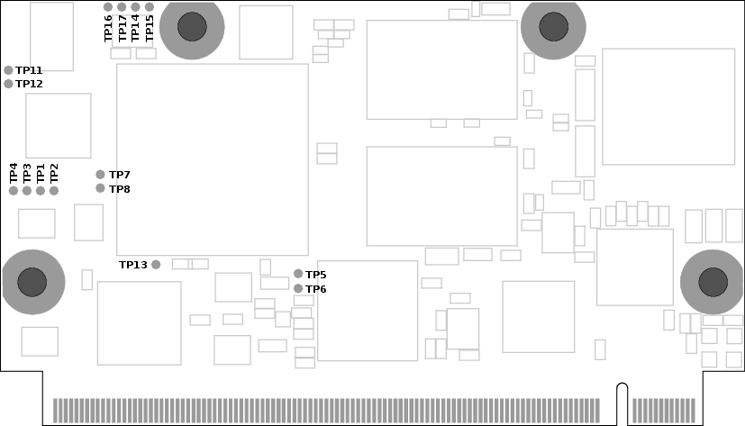
Testpoints on the module
| Testpoint | Name | Description |
|---|---|---|
| TP1 | S_JTAG_MS | CPU PL5 (OpenRISC JTAG) |
| TP2 | S_JTAG_CK | CPU PL6 |
| TP3 | S_JTAG_DO | CPU PL7 |
| TP4 | S_JTAG_DI | CPU PL8 |
| TP5 | UART_DBG_TX | CPU PH20 (CPU UART) |
| TP6 | UART_DBG_RX | CPU PH21 |
| TP7 | STM32_DBG_TX | Cortex-M0 extra UART |
| TP8 | STM32_DBG_RX | Cortex-M0 extra UART |
| TP9 | STM32_USB_N | Internal Full-Speed USB connection |
| TP10 | STM32_USB_P | Internal Full-Speed USB connection |
| TP11 | SWDIO | Cortex-M0 SWDIO |
| TP12 | SWCLK | Cortex-M0 SWCLK |
| TP13 | CLK_OUTA | CPU PA15 |
| TP14 | RISC_TX | CPU PL2 (OpenRISC UART) |
| TP15 | RISC_RX | CPU PL3 |
| TP16 | VCC_PMIC | PMIC always-on voltage |
| TP17 | GND | Ground |
4.6. Electrical Specification
4.6.1. Power Supply
The power supply requirements are listed in the table below and are identical to the Qseven specification.
If the base board does not provide standby power, VCC_5V_SB must be tied to VCC.
| Rail | Description | Nominal voltage | Tolerance |
|---|---|---|---|
| VCC | Main power supply | 5V | 4.75 ... 5.25V |
| VCC_5V_SB | Standby power supply | 5V | 4.75 ... 5.25V |
| VCC_RTC | Backup battery | 3V | 2.4 ... 3.3V |